
 |
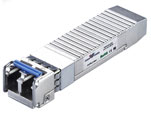
The OP-SFP  -LP-10 series single-mode transceivers are SFPmodule for bi-directional
serial optical data communications such as 10GBASE-SR and 10GBASE-SW.
It is with the SFP20-pin connector to allow hot plug capability. Digital diagnostic functions
are available via an I2C. This module is designed for multi-mode fiber and operates at a
nominal wavelength of 1310 nm.
The transmitter section uses a 1310 nm multiple quantum well DFB laser and is a class1
laser compliant according to International Safety Standard IEC-60825. The receiver section
uses an integrated InGaAs detector preamplifier (IDP) mounted in an optical header and
a limiting post-amplfier IC. -LP-10 series single-mode transceivers are SFPmodule for bi-directional
serial optical data communications such as 10GBASE-SR and 10GBASE-SW.
It is with the SFP20-pin connector to allow hot plug capability. Digital diagnostic functions
are available via an I2C. This module is designed for multi-mode fiber and operates at a
nominal wavelength of 1310 nm.
The transmitter section uses a 1310 nm multiple quantum well DFB laser and is a class1
laser compliant according to International Safety Standard IEC-60825. The receiver section
uses an integrated InGaAs detector preamplifier (IDP) mounted in an optical header and
a limiting post-amplfier IC. |
 |
Operating data rate up to 10.3Gbps |
|
1310 nm DFB-LD Transmitter |
|
Distance up to 10Km |
|
Single 3.3V Power supply and TTL Logic Interface |
|
Duplex LC Connector Interface |
|
Hot Pluggable |
|
Operating Case Temperature Standard: 0°C~+70°C |
|
Compliant with MSA SFP Specification |
|
Digital diagnostic monitor interface |
|
10G Ethernet at 10.3125Gbps |
|
Compatible with SFF-8472 |
| Feature | Standard | Performance |
Electrostatic Discharge (ESD) to the Electrical Pins |
MIL-STD-883E Method 3015.7 | Class1(>500 V) Isolation with the case |
Electromagnetic Interference (EMI) |
FCC Part 15 ClassB | Compatible with standards |
| Laser Eye Safety | FDA 21CFR 1040.10 and 1040.11 EN60950, EN (IEC) 60825-1,2 |
Compatible with Class I laser product. Compatible with TüV standards |
| Component Recognition | UL and CUL | Compatible with UL standards |
| Green Products | RoHS | RoHS6 |
Absolute Maximum Ratings
|
Recommended Operating Conditions
| Parameter | Symbol | Min. | Typical | Max. | Unit | ||
| Operating Case Temperature |
|
0 | + 70 | °C | |||
| Power Supply Voltage | Vcc | 3.15 | 3.3 | 3.45 | V | ||
| Power Supply Current |
Icc | 300 | mA | ||||
| Surge Current | ISurge | +30 | mA | ||||
| Baud Rate | 10.3125 | 10.5 | GBaud |
| TRANSMITTER |
| Parameter | Symbol | Min. | Typical | Max. | Unit | notes |
| CML Inputs(Differential) |
Vin | 150 | 1200 | mVp | AC coupled inputs | |
| Input Impedance (Differential) |
Zin | 85 | 100 | 115 | ohms | Rin> 100 kohms @ DC |
| Tx_DISABLE Input Voltage - High |
2 | 3.45 | V | |||
| Tx_DISABLE Input Voltage - Low |
0 | 0.8 | V | |||
| Tx_FAULT Output Voltage -- High |
2 | Vcc+0.3 | V | Io = 400µA; Host Vcc |
||
| Tx_FAULT Output Voltage -- Low |
0 | 0.5 | V | Io = -4.0mA |
|
|||||||||||||||||||||||||||||||||||||||||
|
|
||||||||||||||||||||||||||||||||||||||||||||||||||||||||||||||||||||||||||||||||||||||
|
|
|||||||||||||||||||||||||||||||||||||||||||||||||||||||||||||
|
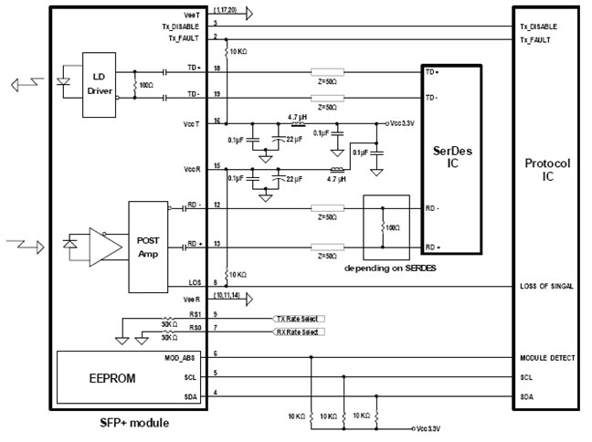
Transceiver Electrical Pad Layout
Pin Function Definitions
| Pin No. | Name | FUNCTION | Plug Seq. | Notes |
| 1 | VeeT | Transmitter Ground | 1 | |
| 2 | TX Fault | Transmitter Fault Indication | 3 | Note 1 |
| 3 | TX Disable | Transmitter Disable | 3 | Note 2, Module disables on high or open |
| 4 | SDA | Module Definition 2 | 3 | Note 3, Data line for Serial ID. |
| 5 | SCL | Module Definition 1 | 3 | Note 3, Clock line for Serial ID. |
| 6 | MOD-ABS | Module Definition 0 | 3 | Note 3 |
| 7 | RS0 | RX Rate Select (LVTTL). | 3 | This pin has an internal 30k pull down to ground. A signal on this pin will not affect module performance. |
| 8 | LOS | Loss of Signal | 3 | Note 4 |
| 9 | RS1 | TX Rate Select (LVTTL). | 1 | This pin has an internal 30k pull down to ground. A signal on this pin will not affect module performance. |
| 10 | VeeR | Receiver Ground | 1 | Note 5 |
| 11 | VeeR | Receiver Ground | 1 | Note 5 |
| 12 | RD- | Inv. Received Data Out |
3 | Note 6 |
| 13 | RD+ | Received Data Out |
3 | Note 7 |
| 14 | VeeR | Receiver Ground | 1 | Note 5 |
| 15 | VccR | Receiver Power | 2 | 3.3±5%, Note 7 |
| 16 | VccT | Transmitter Power | 2 | 3.3±5%, Note 7 |
| 17 | VeeT | Transmitter Ground |
1 | Note 5 |
| 18 | TD+ | Transmit Data In | 3 | Note 8 |
| 19 | TD- | Inv. Transmit Data In |
3 | Note 8 |
| 20 | VeeT | Transmitter Ground |
1 | Note 5 |
| 1 | TX Fault is an open collector/drain output, which should be pulled up with a 4.7K -10K  resistor on the host board. Pull up voltage between 2.0V and VccT, R+0.3V. resistor on the host board. Pull up voltage between 2.0V and VccT, R+0.3V.When high, output indicates a laser fault of some kind. Low indicates normal operation. In the low state, the output will be pulled to < 0.8V. |
| 2 | TX disable is an input that is used to shut down the transmitter optical output. It is pulled up within the module with a 4.7 - 10 K resistor. Its states are:Low (0 - 0.8V): Transmitter on (>0.8, < 2.0V): Undefined High (2.0 - 3.465V): Transmitter Disabled Open: Transmitter Disabled |
| 3 | Modulation Absent, connected to VEET or VEER in the module. |
| 4 | LOS (Loss of Signal) is an open collector/drain output, which should be pulled up with
a 4.7K - 10K resistor. Pull up voltage between 2.0V and VccT, R+0.3V. When high,
this output indicates the received optical power is below the worst-case receiver
sensitivity (as defined by the standard in use). Low indicates normal operation. In
the low state, the output will be pulled to < 0.8V. |
| 5 | VeeR and VeeT may be internally connected within the SFP module. |
| 6 | RD-/+: These are the differential receiver outputs. They are AC coupled 100
differential lines which should be terminated with 100 (differential) at the user
SERDES. The AC coupling is done inside the module and is thus not required on
the host board. The voltage swing on these lines will be between 370 and 2000 mV
differential (185 -1000 mV single ended) when properly terminated. |
| 7 | VccR and VccT are the receiver and transmitter power supplies. They are defined
as 3.3V ±5% at the SFP connector pin. Maximum supply current is 300mA.
Recommended host board power supply filtering is shown below. Inductors with
DC resistance of less than 1 ohm should be used in order to maintain the required
voltage at the SFP input pin with 3.3V supply voltage. When the recommended
supply-filtering network is used, hot plugging of the SFP transceiver module will
result in an inrush current of no more than 30mA greater than the steady state value.
VccR and VccT may be internally connected within the SFP transceiver module. |
| 8 | TD-/+: These are the differential transmitter inputs. They are AC-coupled, differential
lines with 100 differential termination inside the module. The AC coupling is done
inside the module and is thus not required on the host board. The inputs will accept
differential swings of 500 - 2400 mV (250 - 1200mV single-ended), though it is
recommended that values between 500 and 1200 mV differential (250 - 600mV
single-ended) be used for best EMI performance. |
The serial interface uses the 2-wire serial CMOS EEPROM protocol defined for the
ATMEL AT24C02/04 family of components. When the serial protocol is activated, the
host generates the serial clock signal (SCL). The positive edge clocks data into those
segments of the EEPROM that are not write protected within the SFP transceiver. The
negative edge clocks data from the SFP transceiver. The serial data signal (SDA)
is bi-directional for serial data transfer. The host uses SDA in conjunction with SCL to
mark the start and end of serial protocol activation. The memories are organized as a
series of 8-bit data words that can be addressed individually or sequentially.
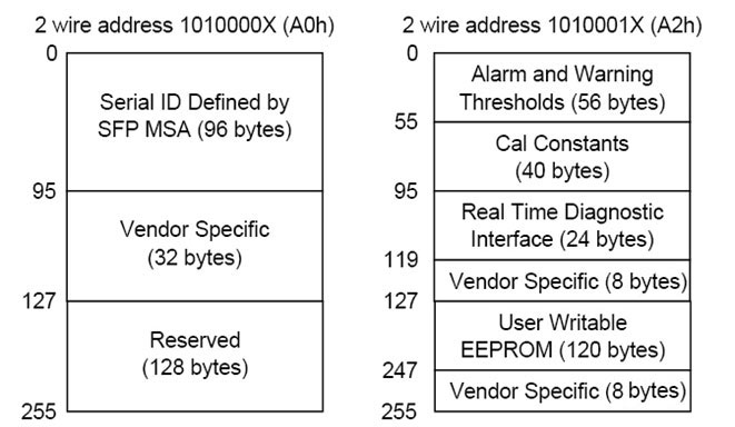
The Module provides diagnostic information about the present operating conditions. The transceiver generates this diagnostic data by digitization of internal analog signals. Calibration and alarm/warning threshold data is written during device manufacture. Received power monitoring, transmitted power monitoring, bias current monitoring, supply voltage monitoring and temperature monitoring all are implemented. The diagnostic data are raw A/D values and must be converted to real world units using calibration constants stored in EEPROM locations 56 - 95 at wire serial bus address A2h. The digital diagnostic memory map specific data field define as following .For detail EEPROM information, please refer to the related document of SFF 8472 Rev 10.2 .
Recommend Circuit Schematic
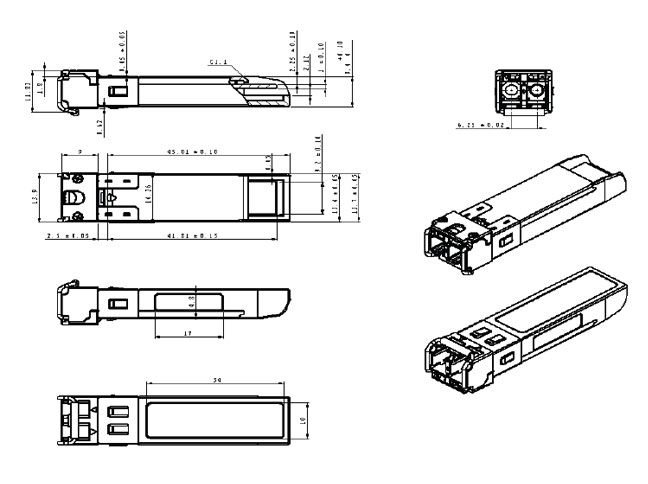
Mechanical Specifications
| Part No. | Data Rate | Laser | Fibre Type | Distance | Optical Interface |
DDMI |
| OP-SFP-LP-10 |
10.3Gbps | 1310nm DFB |
SMF | 10Km | LC | YES |
*I--- Industrial operating temperature
*D--- DDMI
Optiplus Networks reserves the right to make changes to or discontinue any optical link product or service identified in this publication, without notice, in order to improve design and/or performance. Applications that are described herein for any of the optical link products are for illustrative purposes only. Optiplus networks makes no representation or warranty that such applications will be suitable for the specified use without further testing or modification.
| DESCRIPTION | Type | |||
| OP-SFP-LP-10 10.3Gbps SFPTransceiver |
|
New Products
 c
c
 us
us